Navigation auf uzh.ch
Navigation auf uzh.ch
Our research focuses on topological phases of classical and quantum matter. Topological matter exhibits properties resilient against a broad range of perturbations, and include phenomena such as quantized Hall conductivity in semiconductor devices or spin-momentum-locked metallic states on the surface of topological insulators.
We use diverse mathematical techniques and numerical approaches to extend the notion of topological invariants to a broader array of physical systems and to study their fingerprints in physical observables, and we propose prospective setups for realizing them in experiments. Besides conventional crystalline solids, we also explore dissipative and periodically driven systems, along with lattices that feature unique curved or aperiodic geometries.
Spectra and topology in hyperbolic lattices
Curved spaces constitute an essential ingredient of general relativity. As a theoretical tool, negatively curved anti-de Sitter spaces also arise by virtue of a holographic correspondence when describing certain strongly correlated conformal field theories. While curvature of space is not an essential ingredient of traditional condensed matter physics, recent experimental works with superconducting waveguide resonators and with electric-circuit networks made it possible to engineer classical and quantum Hamiltonians with emergent negative curvature. However, little is presently known about generalizations of common condensed matter physics notions, such as crystal symmetry, Bloch band theory, and topological order, to the realm of negatively curved spaces.
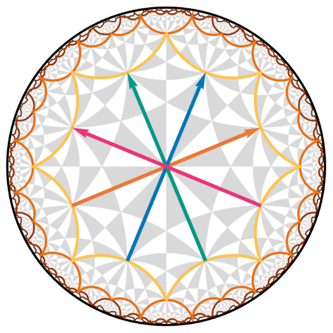
Our group conducted investigations aimed at providing the theoretical characterization of these recent experimental works. We studied the symmetry group of regular “ { p, q }” hyperbolic lattices, where q regular p-gons meet at each vertex. Their spectral and quantum mechanical properties imply unique challenges, owing to the curvature-induced noncommutativity of hyperbolic translations, and practical approaches for efficient computations of their spectra have remained missing. In a work carried out with our former doctoral student Patrick Lenggenhager, we have developed an approach, based on constructing ever larger supercells as symmetric aggregates of smaller cells, that allows for computing hyperbolic spectra with an unprecedented level of detail. To make these tools available for the broader community, we have implemented the technique in a pair of complementary software packages, namely HYPERCELLS for GAP and HYPERBLOCH for Mathematica.
Figure: Hyperbolic {8, 3 } lattice, drawn in the Poincaré disk projection. The indicated primitive unit cell (yellow) tiles the hyperbolic plane, with translation group generated by four primitive translation (colored arrows). The growing supercells (shades of brown) form a coherent sequence that facilitates an efficient computation of energy spectra.
A particularly striking feature of hyperbolic lattices is the high dimension of their reciprocal space. In particular, topological invariants characterizing Euclidean crystals in arbitrarily high spatial dimension, such as the second Chern number describing non-linear quantum Hall state in four-dimensional space, can arise in two-dimensional hyperbolic lattice. By leveraging the supercell method, we currently investigate how these exotic topological states are constrained by crystalline symmetry, and how they manifest through bulk-boundary correspondence and in transport properties.
Highlighted Publications:
We study topological phases of quantum matter with numerical and analytical tools. Topological electronic states are characterized universal and robust phenomena, such as the Hall conductivity in the integer quantum Hall effect, that are of fundamental interest or promise applications in future electronics. We study and propose concrete materials to realize such topological effects, but are also interested in studying abstract models to understand what phases of matter can exist in principle.
Our numerical toolbox includes neural network algorithms to study strongly interacting quantum many-body systems. Furthermore, we work at the interface of quantum computing and condensed matter physics.
Building topological crystalline superconductors atom by atom Two-dimensional superconductors are a highly sought-after phase of matter, and their fundamental characteristic is the presence of Majorana modes at their boundaries. While these phases are elusive in natural compounds, they may be realized by designing artificial quantum materials. Our group has worked closely with researchers in the Sessi group at the Max Plank Institute of Microstructure Physics in Halle, Germany, to build a platform in which such exotic superconductivity can be found. The workhorse are socalled Shiba-states, which appear when a magnetic atom (in our case chromium) is added to the surface of a conventional superconductor (in our case niobium). The Shiba states are located near the magnetic adatom in the spectral gap of the superconductor. Adding several atoms next to each other will lead to a hybridization of their Shiba states. If a whole lattice of adatoms is formed, one can think of a “band structure” of Shiba states — all within the gap of the underlying superconductor and thus at very low energies. This band structure is by construction that of a superconductor and can be in different topological phases, depending on the design of the lattice. By assembling the lattices of magnetic adatoms one by one, using scanning tunnelling microscopy techniques, it was possible to built different two dimensional structures, distinguished by the type of lattice in the bulk and termination geometry. Scanning tunnelling microscopy also allows to probe these structures with single-atom precision. The experimental measurements and theoretical predictions indicate that two of the structures host Majorana edge bands and corner Majorana modes, respectively, which are protected by the crystalline symmetries of the sample and termination geometry. The corner Majorana modes are a manifestation of the concept of “higher-order topology” that was introduced by our group in 2018. Standard topological phases host special protected modes on their boundary (a surface for threedimensional systems and an edge for two-dimensional systems). Higher-order topological phases exhibit such modes in lower-dimensional sections of the boundary (a hinge of a three-dimensional system and a corner for a twodimensional system). So far, experiments have focused on realizing higher-order topology in three-dimensional semiconductors and two-dimensional metamaterial structures. Our study reports the first realization of higher-order topology in superconductors. This work shows that Shiba lattices are a promising a platform to design topological phases in two dimensional superconductors.
Highlighted Publications:
N. Shumiya et al. Nature Materials 21, 1111–1115 (2022)
We investigate quantum matter phases emerging from strong electronic interactions. High-temperature superconductivity, strange metals, density-wave instabilities and electronic driven metal insulators metal-insulator transitions are studied by synchrotron techniques. Using angle-resolved photo-emission spectroscopy (ARPES) and resonant inelastic x-ray scattering (RIXS), we reveal electronic structures and properties of such correlated electron systems. Quantum phase transitions tuned by magnetic field, uniaxial or hydrostatic pressure are furthermore explored by high-energy x-ray diffraction. Our group also has technical initiatives to develop innovative and compact cryo-cooling methodology. Finally, we are involved in data science analysing x-ray scattering results using machine learning methodology.
Hallmarks of quantum matter are complex phases emerging from electronic interactions. An experimental progress pathway is to study these phases with advanced spectroscopy techniques. Here, we provide two study examples using electron spectroscopy and resonant x-ray scattering on, respectively, a multi-orbital Mott insulator and a superconductivity charge order system.
Skin metal-insulator transition
Doped Mott insulators are the starting point for interesting physics such as high temperature superconductivity and quantum spin liquids. For multi-band Mott insulators, orbital selective ground states have been envisioned. However, orbital selective metals and Mott insulators have been difficult to realize experimentally. Using photoemission spectroscopy, we demonstrated how Ca2RuO4 , upon alkali-metal surface doping, develops a single-band metal skin. Our dynamical mean field theory calculations reveal that homogeneous electron doping of Ca2RuO4 results in a multi-band metal. All to gether, our results provide evidence for an orbital-selective Mott insulator breakdown, which is unachievable via simple electron doping. Supported by a cluster model and cluster perturbation theory calculations, we demonstrate a type of skin metal-insulator transition induced by surface dopants that orbital-selectively hybridize with the bulk Mott state and in turn produce coherent in-gap states.
Charge order and superconductivity
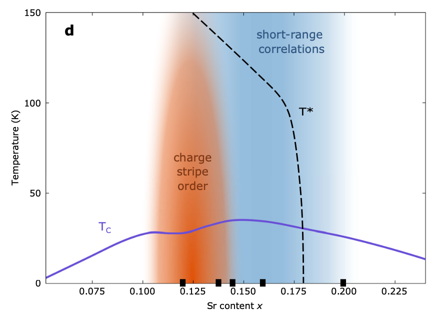
In high-temperature cuprate superconductors, stripe order refers broadly to a coupled spin and charge modulation with a commensuration of eight and four lattice units, respectively. How this stripe order evolves across optimal doping remains a controversial question. Here we carried out a systematic resonant inelastic x-ray scattering (RIXS) study of weak charge correlations in La2−xSrxCuO4 and La1.8−xEu0.2SrxCuO4 . Our ultra high energy resolution experiments demonstrate the importance of the separation of inelastic and elastic scattering processes. Long-range temperature-dependent stripe order is only found below optimal doping. At higher doping, short-range temperature-independent correlations are present up to the highest doping measured. This transformation is distinct from and preempts the pseudogap critical doping. We argue that the doping and temperatureindependent short-range correlations originate from unresolved electron–phonon coupling that broadly peaks at the stripe ordering vector.
Spin-off initiative
After winning the Swiss Innovation Award end of 2021, condenZero matured – in 2023 – to the level where the company could move to the Zurich-campus. The patent underlying the company technology went into the nationalization phase (accepted in China, pending decision in EU, USA, Canada). Three orders arrived in 2023 and Innosuisse awarded a "consolidation" innovation grant.
Highlighted Publications:
K. von Arx et al., npj Quantum Materials 8, 7 (2023)
M. Horio et al., Communications Physics 6, 323 (2023)
Our group is dedicated to the growth and investigation of transition metal oxide heterostructure (i.e. thin films, superlattices). The ability to create structures with sub-nm precision by off-axis rf magnetron sputtering allows us to tune the properties of these materials thanks to reduced dimensionality and interface reconstructions. Our goal is to understand the subtle atomic-scale structural and electronic mechanisms controlling interface physics in complex oxides, which is key for the rational design of materials with tailored properties.
Transition metal oxides are a fascinating and widely studied class of materials displaying a wide range of physical properties (i.e. metal-insulator transitions, magnetism, superconductivity, etc.) useful for the development of next-generation electronic devices. All these functionalities stem from strong electronic correlations and a complex interplay between the charge, orbital, spin and lattice degrees of freedom. The generation of thin films and heterostructures allows these functionalities to be tuned even further, i.e. by imposing epitaxial strain and lowering the dimensionality. For instance, we recently showed that B-site ordered double perovskite Nd2NiMnO6 films exhibit ferromagnetism even at ultralow thicknesses of only 3 unit cells (≈1.2 nm). Through a detailed x-ray magnetic circular dichroism study, we were able to distinguish the magnetic components into a strong ferromagnetic Ni/Mn sublattice and a paramagnetic Nd sublattice. In Zurich, we continued the investigation of SrCrO3 thin films. Transport measurements have revealed a metallic phase down to 100K for films grown under low strain with a strain-dependent metal-to-insulator transition. On the other hand, magnetic properties measurements revealed a strainindependent antiferromagnetic phase at temperatures below 150K. These findings prove the coexistence of an antiferromagnetic and metallic phase in SrCrO3 films. The possible Fermi surface reconstruction occurring at the metal-insulator transition signalled by a change in charge carrier is currently being investigated using magnetoresistance measurements. In parallel, we started the fabrication and investigation of superlattices alternating ultrathin layers of SrCrO3 and LaCrO3. In contrast to SrCrO3, LaCrO3 is known to be insulating and weakly ferromagnetic. As both materials stabilise with different oxidation states, a polar discontinuity occurs at the interfaces between SrCrO3 and LaCrO3 together with interfacial charge transfer. Scanning transmission electron microscopy measurements are used to investigate the microscopic atomic structure of the superlattices, revealing coherent and epitaxial growth and a low intermixing at the layer interface. The SrCrO3/ LaCrO3 superlattices have a rather small resistivity. They show a metallic behaviour with two resistivity upturns when the SCO layer is thicker than 16uc but only one when less than 5uc.
Highlighted Publications:
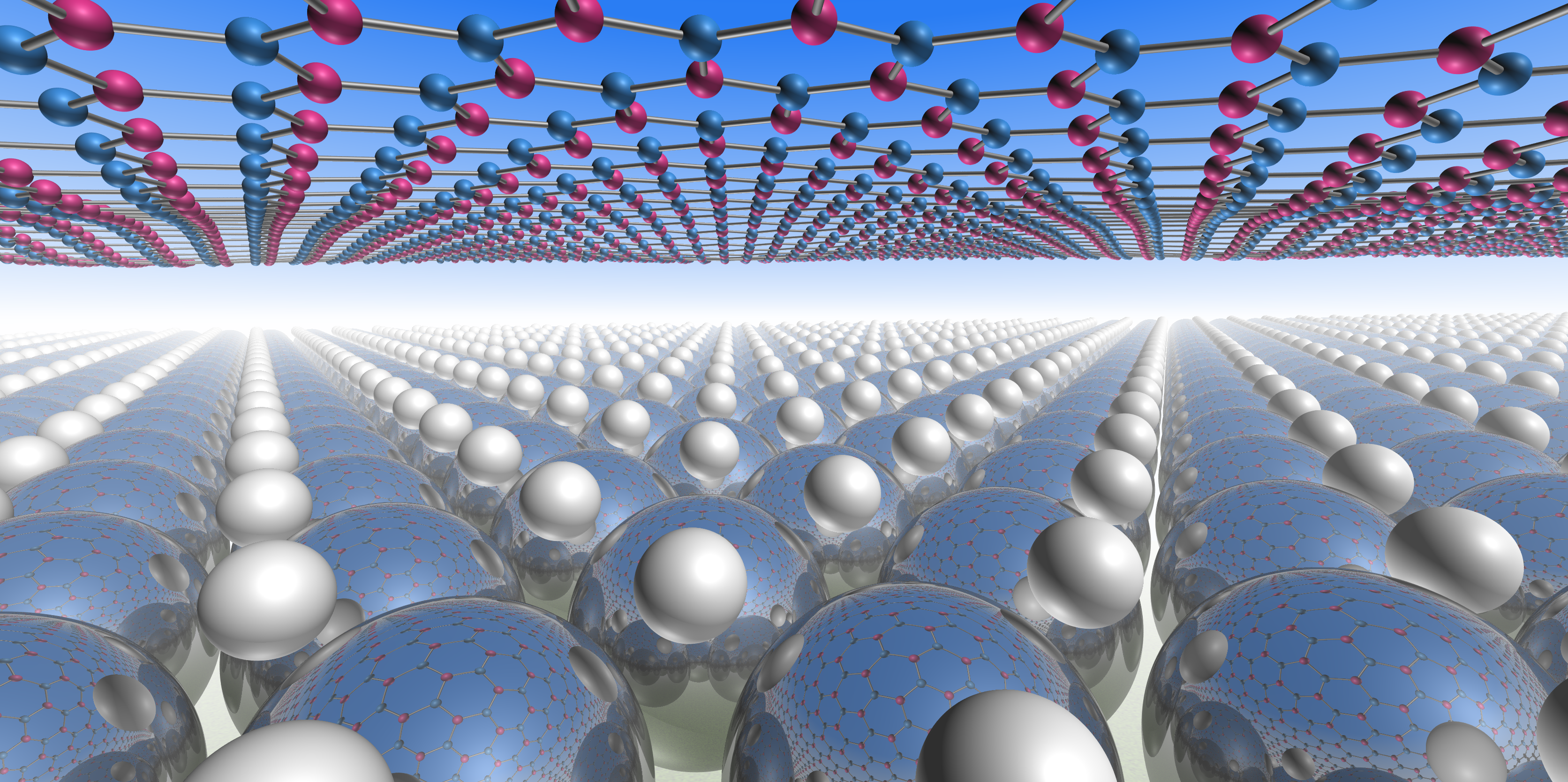
We study objects like zero-dimensional endofullerene molecules and two-dimensional (2D) boron nitride layers in view of their functionality as nano-materials. Single-molecule magnetism is the focus of the fullerene research, where we apply x-ray absorption and a subKelvin superconducting quantum interference device. In the activity of the 2D materials, we grow the highest quality boron nitride on substrates up to the four-inch wafer scale with chemical vapor deposition, subsequent exfoliation, and implementation in devices. At UZH Irchel, we use a dedicated clean room, optical microscopy, inkjet printing, and surface science tools such as low-energy electron diffraction, photoemission, and scanning tunneling microscopy for these purposes. At the Swiss Light Source, we perform photoemission and x-ray absorption spectroscopy experiments.
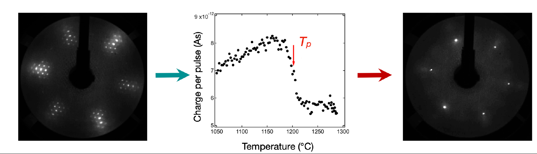
Stability of single layer h-BN on metals
High quality single layer hexagonal boron nitride may be grown on transition metals with chemical vapor deposition (CVD). These systems are used as templates for molecules, production of pores with nanometer size, functional electrodes in electrochemical cells, or as educts for the production of free standing boron nitride layers. With density functional theory (DFT) we calculated the atomic adsorption energies of boron and nitrogen, BN dimers, (BN)3 hexamers and h-BN with and without atomic vacancies for different transition metals. It turns out that the catalytic substrates lower the stability of the h-BN that is e.g. more stable on copper than on nickel. Importantly, defects, impurities like carbon or domain boundaries lower the stability of the systems. The over all stability may be quantified with pyrolysis experiments where the systems are heated at a given rate to high temperatures. The disintegration of the h-BN is measured in the decrease of the photoelectron yield of a xenon flash lamp. For the case of h-BN on platinum the Figure shows high quality electron diffraction pattern of h-BN on Pt(111) before and clean Pt(111) after heating. The record pyrolysis temperature Tp of 1200 ◦C indicates highest quality boron nitride. The pyrolysis temperature of h-BN on a given transition metal is a measure for its quality and can be correlated to the DFT results. The calculations run at the at the Swiss National Supercomputing Centre (CSCS) in Lugano, and the experiments were performed in the Sinergia lab on the Irchel campus of the University of Zürich. The project was funded by the European Commission (European Union’s Horizon 2020 research and innovation programme) under the Graphene Flagship.

Highlighted Publications:
Our research is centered on genuine quantum phenomena in bulk materials that arise due to collective electronic behavior. These electronic correlations strongly couple spin, charge and lattice degrees of freedom resulting in emergent and rich low-energy physics. We study materials in which such collective quantum phenomena at the atomic-scale are borne out in exotic and functional macroscopic properties. We tune the underlying quantum interactions via external control parameters (pressure, field, strain, crystal chemistry) to understand the properties of quantum materials. For this purpose, we probe quantum matter with state-of-the-art large-scale neutron, photon and muon experiments.
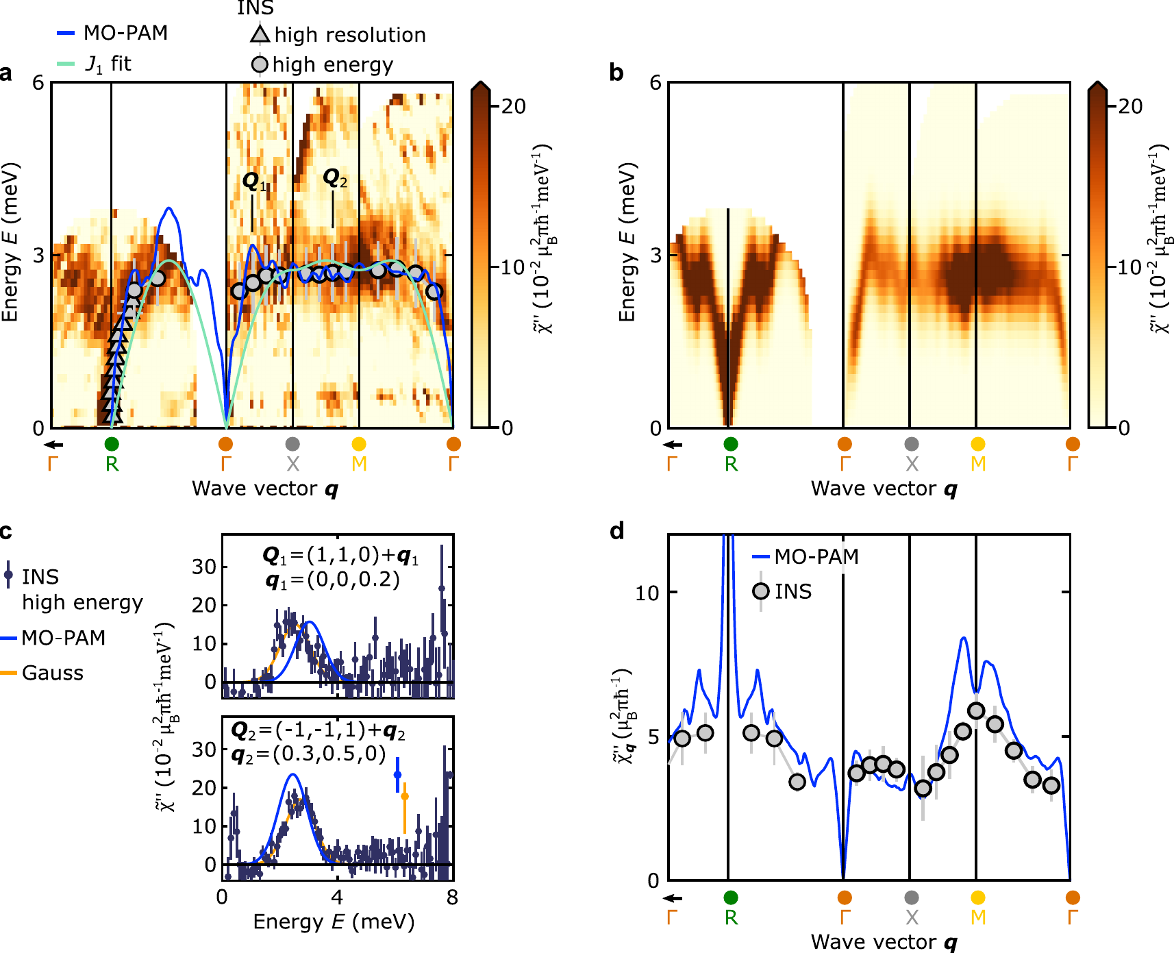
A quantitative Kondo Lattice Model Electrons at the border of localization generate exotic states of matter across all classes of strongly correlated electron materials and many other quantum materials with emergent functionality. The Kondo lattice model has been key in qualitatively demonstrating how a myriad of correlated quantum matter states emerge from the interplay of local and itinerant electrons. Beyond the strongly correlated electron materials for which this archetypal model was conceived, it applies to a growing list of novel quantum systems with potential for applications including the electronic transport through quantum dots, voltage-tunable magnetic moments in graphene, magnetism in twisted-bilayer graphene and in two-dimensional organometallic materials, the electronic structure in layered narrow-electronic-band materials, electronic resonances of Kagome metals, metallic spin liquid states, skyrmions in centrosymmetric magnets and fully tunable electronic quasiparticles in semiconductor moiré materials. Further, Kondo lattice models have been used to study flat-band materials and predict novel topological states such as topological superconductivity and quantum spin liquid states, including the highly sought-after fractional quasiparticles. Despite this continued relevance, quantitative predictions for real materials based on Kondo lattice models remain a formidable computational hurdle. Both for experiment and theory, the challenge in understanding real materials is the extreme energy resolution required to capture the inherently small energy scales that emerge in the renormalized electronic state arising from interplay of local and intinerant electrons. Notably, materialsspecific theoretical investigations of emergent phenomena are often limited by the difficulty of validating low-energy effective models derived from complex high-energy input. Together with our theory collaborators from the University of Tennessee, Los Alamos, and RIKEN, we have demonstrated that for the prototypical strongly-correlated antiferromagnet CeIn3 a multi-orbital periodic Anderson model embedded with input from ab initio bandstructure calculations can be reduced to a simple Kondo-Heisenberg model, which captures the magnetic interactions quantitatively. We validate this tractable Hamiltonian via high-resolution neutron spectroscopy that reproduces accurately the magnetic soft modes in CeIn3 (see figure), which are believed to mediate unconventional superconductivity. Our study paves the way for a quantitative understanding of metallic quantum states such as unconventional superconductivity.
Highlighted Publications:
Our research group focuses on low-dimensional quantum materials. We explore how matter receives her properties from the interaction between individual atoms and molecules using atomically resolved scanning probe microscopy (SPM). By subjecting matter to extreme conditions - such as cryogenic temperatures, exposure to magnetic fields, or doping – we find control knobs that finetune material properties. Our investigations include measurements of the electronic structure using SPM enabled electron spin resonance, pump-probe spectroscopy, and fast quasiparticle interference imaging.
Electronic Structure Mapping of 2D Materials
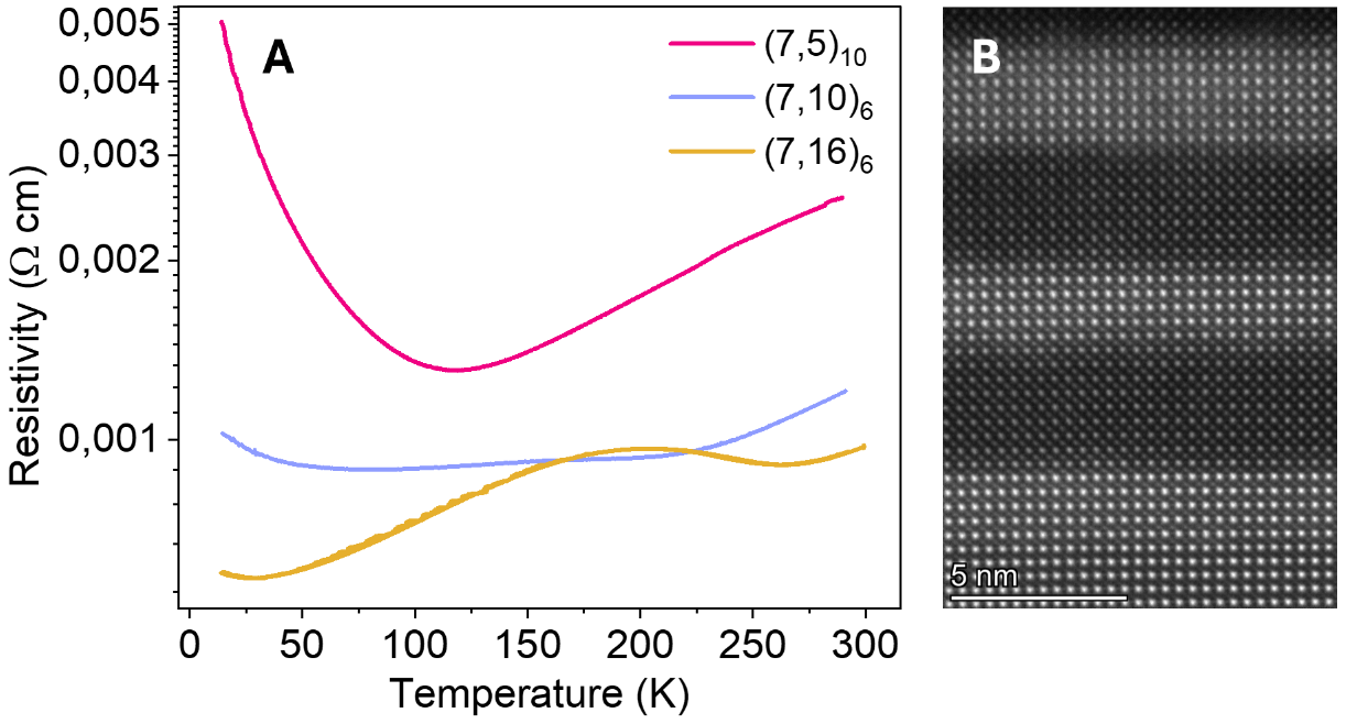
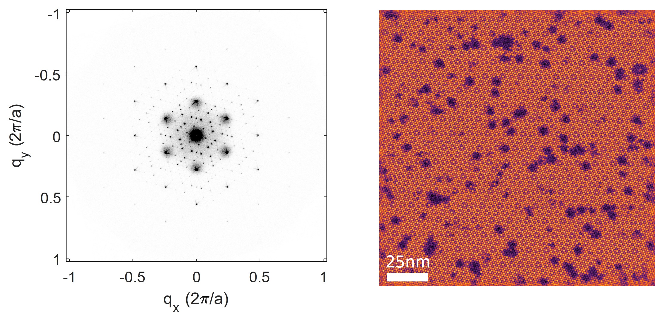
We infer the band structure of two dimensional quantum materials using fast quasiparticle interference imaging (QPI). QPI works by measuring the point spectroscopy (local density of states) at every topographic location. To speed up this traditionally slow technique, we utilize compressed sensing and parallel spectroscopy. While the former enables the measurement of fewer locations, the latter speeds up the LDOS mapping. Using our fast QPI method, we investigate the van der Waals material 4Hb-TaS2 that exhibits a superlattice of alternating layers with 1H and 1T coordination structures. The interaction between the two charge density waves (CDW) of the respective layers enhances the superconducting properties compared to pristine 2H-TaS2. We identify a weakly dispersing band on the 1T surface and find domains with different orientations of the CDW, which change the observed long-wavelength Moiré patterns at the surface and the energy onset of the weakly dispersing band.
Superconducting tips for Josephson Junction
STM To enhance the energy resolution of our STM, we introduce a straightforward method to create superconducting tips made from Nb wires. The trick is to controllably break the Nb wires in vacuum to expose fresh metal to the vacuum instead of ambient pressure that previously resulted in oxidized tips. These superconducting tips can be used for QPI mapping or represent one part of a Josephson junction. The latter act as the central component of a charge qubit that can be scanned along the surface and used to atomically map the presence of sources of decoherence or it provides insight into the pairing mechanism of low-dimensional superconductors via the emission of Josephson radiation.

Highlighted Publications:
Vacuum cleaving of superconducting niobium tips to optimize noise filtering and with adjustable gap size for scanning tunneling microscopy Carolina A. Marques et al., MethodsX 11, 102483 (2023), DOI: 10.1016/j.mex.2023.102483
We are interested in selected topics in materials research, spanning the entire spectrum from searching new materials, their characterization, and corresponding applications. We have been particularly active in superconductivity, magnetism and thermodynamics. Our laboratory is equipped with modern furnaces for material synthesis, 4He/3He cryostats and a dilution cryostat, all with superconducting magnets. We are structuring thin superconducting films at the FIRST Center for Micro- and Nanoscience at ETHZ and are using them both for basic research and applications. Corresponding nanostructures may serve as ultrafast single-photon detectors in the infrared, visible and Xray range.
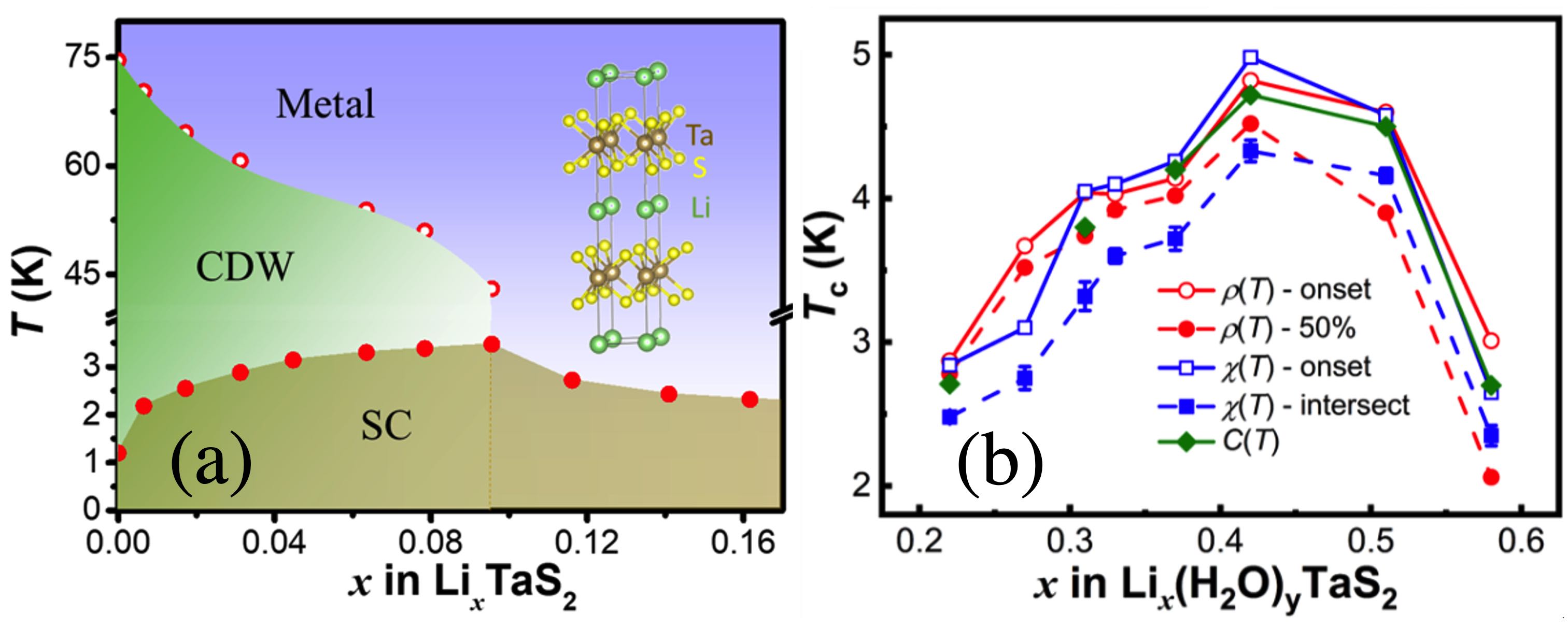
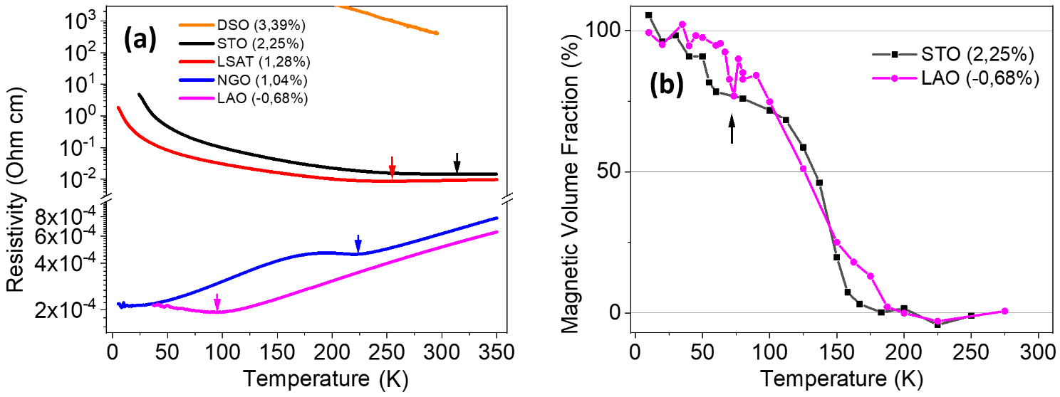
Superconductivity in un-hydrated and hydrated Lix(H2O)yTaS2
Layered transition-metal dichalcogenides (TMDs) have attracted increasing interest due to their relevance in understanding high-temperature superconductors. They can exhibit various quantum states such as metallic, Mott insulating, and a state with charge-density waves (CDWs). 2HTaS2 is a prominent representative member of the 2H-TMD family, in which both superconductivity and CDW can coexist. In bulk 2H-TaS2, the incommensurate charge-density wave order has a transition temperature (TCDW) of approximately 75 K. This state coexists with superconductivity as the temperature decreases below the superconducting transition temperature (Tc) of 0.8 K. Like in other transition metal dichalcogenides, this transition temperature can be tuned through chemical doping, intercalation, annealing, gating, and exfoliation or restacking. We have systematically studied the structural and physical properties of Liintercalated LixTaS2 and hydrated Lix(H2O)yTaS2 (y ≈ 0.86). In un-hydrated LixTaS2, the CDW formation temperature is continuously suppressed by gradually increasing the lithium content x, and Tc increases with a maximum transition temperature Tc = 3.5 K for x = 0.096 (see Fig. a). In contrast, there are no signs of a charge-density wave formation in hydrated Lix(H2O)yTaS2, where the intercalation of water leads to a considerable expansion of the unit cell. There, the transition temperature to superconductivity also shows a dome-shaped dependence on the lithium content x, but with a maximum Tc of 4.6 K for a comparably high Li content (x ≈ 0.42) (Fig. b). This Tc value is larger than that of corresponding optimally doped 2H-TaS2 without water or organic intercalants, which supports the scenario that a weakened interlayer coupling, resulting from a large interlayer spacing, may suppress the tendency of charge-density wave formation and thereby enhances superconductivity. At first glance, the dependence of Tc on the Li content x may be attributed to an associated charge-carrier doping. However, our Hall-effect data taken on LixTaS2 suggest that the changes in the effective number of charge carriers is at least an order of magnitude larger than that inferred from the Li-content x alone. Therefore, the intercalation probably primarily weakens the CDW state and thus indirectly leads to a strong increase in the density of the mobile charge carriers, which in turn promotes superconductivity.
Highlighted Publications:
We develop lens-less imaging methods towards highresolution and three-dimensional imaging of nano-scaled objects, two-dimensional materials and macromolecules. Coherent diffraction imaging and holography are lensless imaging techniques where the intensity of the wave diffracted by the sample is acquired by a detector in the far field. The phase distribution of the diffracted wave together with the sample structure is then reconstructed by applying numerical methods. Employing short wavelength radiation, such as electron or X-ray waves, in lens-less imaging techniques allows for imaging at atomic resolution.
Coherent imaging with low-energy electrons, quantitative analysis
Low-energy electrons (20 - 300 eV) hold the promise for lowdose, non-destructive, high-resolution imaging, but at the price of challenging data analysis. Recently, we quantitatively evaluated the properties of low-energy electrons when applied for coherent imaging [1]. Unlike electrons of energies typically employed in commercial transmission electron microscopes (20 - 300 keV), low-energy electrons (20 - 300 eV) introduce about 10 times larger phase shift into the probing electron waves. The maximal phase shift acquired by a 120 eV electron wave scattered by a carbon atom was theoretically estimated to be 5.03 radian and experimentally measured to be between 3 and 7.5 radian. Low-energy electrons diffract much stronger than high-energy electrons, the corresponding point spread function shows that only very thin objects of up to 3 Å in thickness can be imaged in focus. Thus, when imaging an object of finite thickness, such as a macromolecule, the obtained image will always be blurred due to the out-of-focus signal, which can be an explanation for the long-standing problem of limited resolution in low-energy electron holography of macromolecules. A simple method to quantitatively evaluate the absorption of a specimen from its in-line hologram without the need to reconstruct the hologram was presented.
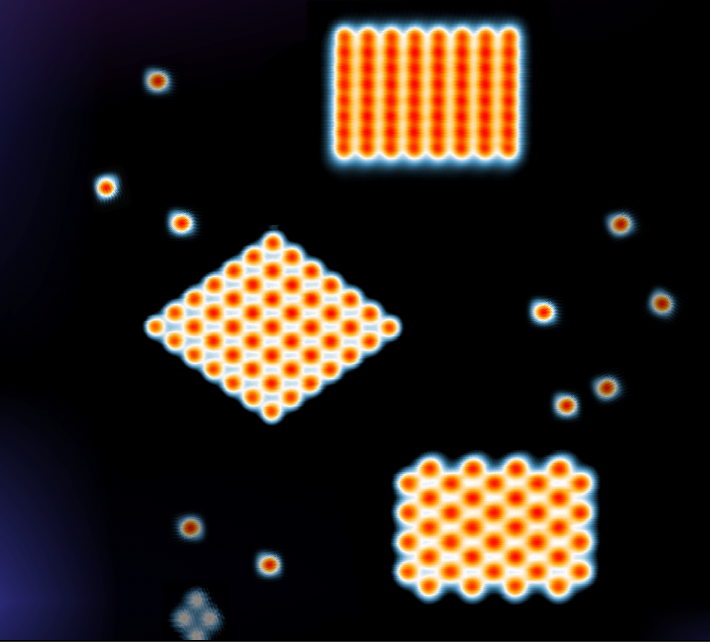
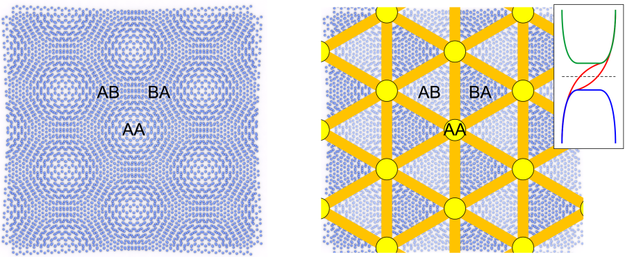
Controlling topological states in bilayer graphene
Topological states are exciting physical objects with potential for use in quantum applications. In bilayer graphene, the topological states are hosted by the domain walls (DWs) that separate the AB and BA stacking of atoms. An example of topological channels in twisted bilayer graphene is shown in Figure 1. The DWs size can be changed by lithium intercalation, but the overall number of DWs is preserved; these processes were visualised by electron microscopy by Endo et al. (Nat. Nanotech. 18, 1154–1161 (2023)). We provided perspective for future directions for such lithium-intercalated systems: The electronic properties of such systems are yet to be characterised. Moreover, other 2D crystals and various intercalating atoms can be tried out. The observed differences in the speed of lithium intercalation and de-intercalation processes can be further investigated; such studies can help in understanding the lithium battery operation processes at the atomic level.

Highlighted Publications:

The group investigates materials and plasmas for enabling new laser concepts. In particular, a main challenge is the realization of compact X-ray lasers. These are complementary to accelerator beamlines or high harmonic generation beamlines. The level of footprint reduction influences the conceptual design. For lab-scale systems, either kiloampere discharges or terawatt laser pulses are used as pumps. For X-ray lasers on a chip, we are exploring 2D materials with resonant capabilities.
Link
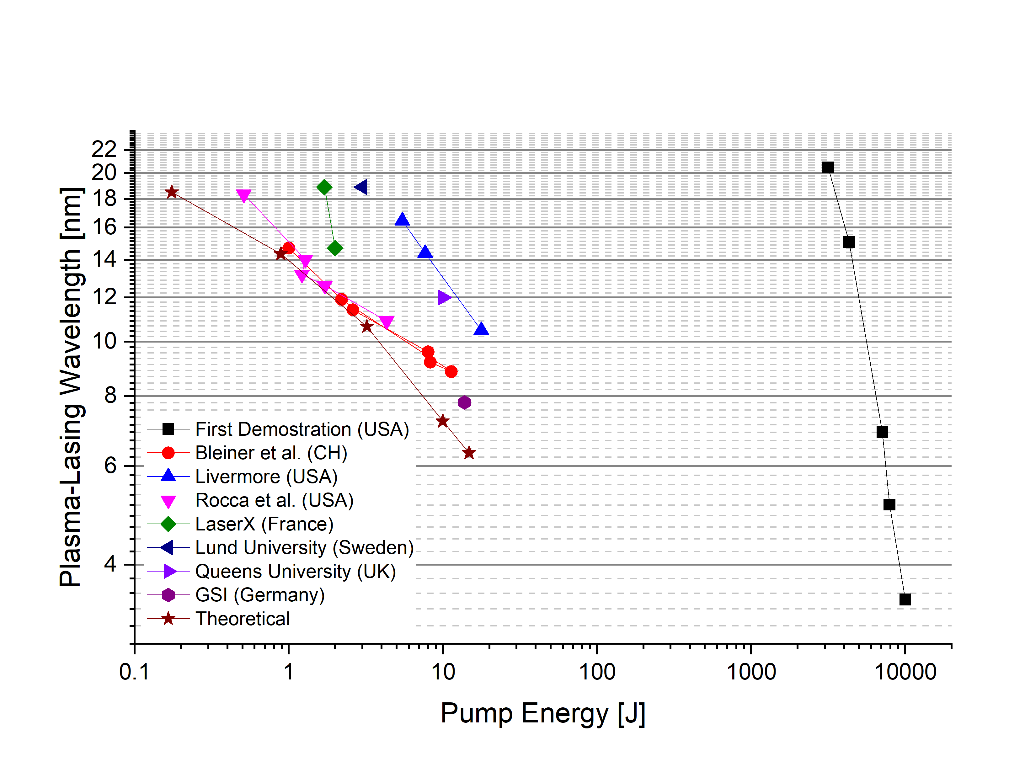
Plasma Physics for Tabletop X-ray Lasers
Plasmas of highly ionized atoms have electronic transition of higher energy than the neutral counterparts found in crystalline lattices. Henceforth, the use of plasmas as gain media permits to realize lasing action at higher transition energies. These are in the VUV down to the soft X-rays. Stimulated emission and amplification across a plasma is a single-pass process, without resonator.
The main challenge is that the plasma is not as homogeneous as a crystal medium. From the early days at Livermore National Laboratory with multi kJ pulses, the efficiency has dramatically grown to fit of a optical table in the lab. Typically, electrical discharges or laser-produced plasmas are used.
Highlighted Publication:


